Microchannel Chip Cooling Technology application in liquid cooling solution
Liquid cooling is the future of data centers. The air cannot handle the power density that reaches the data hall, so a dense fluid with high thermal capacity is flowing into the connection. As the heat density of IT equipment increases, the liquid becomes closer to it. But how far can liquids get close? It is widely accepted to operate a water circulation system through the back door of data center cabinets. Next, the system keeps circulating water to the cold board on particularly hot components such as GPUs or CPUs. In addition, the immersion system sinks the entire rack into the dielectric fluid, so the coolant can come into contact with every part of the system. The main suppliers now offer servers optimized for immersion.

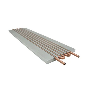
In 1981, researchers David Tuckerman and R F Pease from Stanford University proposed etching tiny "microchannels" into heat sinks to more effectively remove heat. Small channels have a larger surface area and can more effectively remove heat. They suggest that heat sinks can become a component of VLSI chips, and their demonstration demonstrates that microchannel heat sinks can support an impressive heat flux of 800W per square meter.

With the development of semiconductor manufacturing and its entry into three-dimensional structures, the idea of integrated cooling and processing has become more practical. Starting from the 1980s, manufacturers attempted to overlay multiple components on silicon chips. Creating channels on top of multi-layer silicon chips may be a fast and optimal method for cooling, as it can start by simply implementing small grooves similar to fins on a heat sink. But this idea has not received much attention because chip suppliers hope to use 3D technology to stack active components. This method is now accepted by high-density memory, and Nvidia patents indicate that it may be intended to stack GPUs.

Researchers have been working on etching microfluidic channels onto the surface of silicon chips for several years. A team from Georgia Institute of Technology collaborated with Intel in 2015 to potentially be the first to manufacture an FPGA chip with an integrated microfluidic cooling layer, located only a few hundred micrometers away from where the transistor works on silicon. "We eliminated the heat sink on the top of the silicon chip by cooling the liquid only a few hundred micrometers away from the transistor," said Professor Muhannad Bakir, team leader at Georgia Institute of Technology, in a press release. We believe that integrating microfluidic cooling directly and reliably into silicon will become a disruptive technology for the next generation of electronic products.

A 3D network of microfluidic cooling channels has been designed inside the chip, located just a few micrometers below the active part of each transistor device, from where heat is generated. This method can improve cooling performance by 50 times. Microchannels transport fluids directly to hotspots and handle an astonishing power density of 1.7 kW per square centimeter. This is equivalent to 17MW per square meter, which is several times the current GPU heat flux.

The difficulty of heat dissipation means that the largest chips today cannot use all transistors at once, otherwise they will overheat. The application of microfluidics can improve chip performance and efficiency. It is possible to operate data centers more efficiently without the need for energy intensive refrigeration systems.