How to solve the thermal problem of chip packaging
Advanced packaging chips not only meet the needs of high-performance computing, artificial intelligence, power density growth, etc., but also complicate the heat dissipation issues of advanced packaging. Because a hot spot on a chip can affect the heat distribution of adjacent chips. The interconnection speed between chips is also slower in modules than in SoC.

Engineers are searching for effective ways to dissipate heat from complex modules. Placing multiple chips side by side in the same package can alleviate thermal issues, but as the company further delves into chip stacking and denser packaging to improve performance and reduce power, they are battling a series of new issues related to heat.

The current popular flip BGA packaging area with CPU and HBM is approximately 2500 square millimeters. We see that a large chip may become four or five small chips. So it is necessary to have more I/O in order for these chips to communicate with each other. So you can distribute heat. In fact, some devices are so complex that it is difficult to easily replace components in order to customize these devices for specific field applications. This is why many advanced packaging products are used for components with very large quantities or price elasticity, such as server chips.

During the design process, circuit designers may have a concept of the power levels of various chips placed in the module, but may not know whether these power levels are within the reliability range. Therefore, engineers are searching for new methods to conduct thermal analysis of packaging reliability before manufacturing packaging modules. Through thermal simulation, we can understand how heat is conducted through silicon chips, circuit boards, adhesives, TIMs, or packaging covers, while using standard methods such as temperature difference and power function to track temperature and resistance values.
Thermal simulation is the most economical method for exploring the selection and matching of materials. By simulating chips in their working state, we usually discover one or more hotspots, so we can add copper to the substrate below the hotspots to facilitate heat dissipation; Or change the packaging material and add a heat sink.

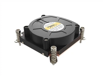
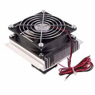
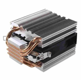
In packaging, over 90% of the heat is dissipated from the top of the chip to the heat sink through the packaging, usually a vertical fin based on anodized aluminum oxide. A thermal interface material (TIM) with high thermal conductivity is placed between the chip and the package to help transfer heat. The next generation TIM for CPUs includes metal sheet alloys (such as indium and tin), as well as silver sintered tin, with conductivity of 60W/m-K and 50W/m-K, respectively.

The initial concept of advanced packaging is that it will work like LEGO building blocks - chips developed at different process nodes can be assembled together, and thermal issues will be alleviated. But this comes at a cost. From the perspective of performance and power, the distance the signal needs to propagate is crucial, and the circuit always remains open or needs to be partially open, which can affect thermal performance. Splitting chips into multiple parts to increase production and flexibility is not as simple as it may seem. Each interconnect in the packaging must be optimized, and hotspots are no longer limited to a single chip.
Early modeling tools could be used to exclude different combinations of chips, providing a great driving force for designers of complex modules. In this era of continuously increasing power density, thermal simulation and the introduction of new TIMs will still be essential.