How to solve the thermal problems of chip packaging
Logic chips generate heat, and the denser the logic and the higher the utilization of the processing elements, the greater the heat. ...
Engineers are looking for ways to efficiently dissipate heat from complex modules.
Placing multiple chips side by side in the same package can alleviate thermal issues, but as companies delve further into chip stacking and denser packaging to increase performance and reduce power, they are battling a new set of heat-related issues .
Advanced packaging chips can not only meet the needs of high-performance computing, artificial intelligence, power density growth, etc., but the heat dissipation issues of advanced packaging have also become complex. Because hot spots on one chip will affect the heat distribution of adjacent chips. The interconnect speed between chips is also slower in modules than in SoCs.
"Before the world got into things like multi-core, you were dealing with a chip that had a maximum power of about 150 watts per square centimeter, which was a single point heat source," said John Parry, head of electronics and semiconductors at Siemens Digital Industries Software. You can dissipate heat in all three directions, so you can achieve some pretty high power densities. But when you have a chip and put another chip next to it, and then put another chip next to it, they "They heat each other up. That means you can't tolerate the same power level for each chip, which makes the thermal challenge much more difficult."
This is one of the main reasons for the slow progress of 3D-IC stacking in the market. While the concept makes sense from a power efficiency and integration perspective - and works well in 3D NAND and HBM - it's a different story when the logic is included. Logic chips generate heat, and the denser the logic and the higher the utilization of the processing elements, the greater the heat.This makes logic stacking rare, which explains the popularity of 2.5D flip-chip BGA and fan-out designs

01 Choose the right package
For chip designers, there are many packaging options. But the performance of chip integration is crucial. Components such as silicon, TSVs, copper pillars, etc. all have different thermal coefficients of expansion (TCE), which affects assembly yield and long-term reliability.
If you open and close at a higher frequency, you may run into thermal cycling issues. The printed circuit board, solder balls, and silicon all expand and contract at different rates. Therefore, it is normal to see thermal cycling failures in the corners of the package, where the solder balls may crack. So one might put an extra ground wire there or an extra power supply.
The currently popular flip-chip BGA package with CPU and HBM has an area of about 2500 square millimeters. "We're seeing one big chip potentially become four or five small chips," said Mike McIntyre, director of software product management at Onto Innovation. "So you have to have more I/O to allow those chips to talk to each other. So you can allocate heat.
Ultimately, cooling is an issue that can be dealt with at the system level, and it comes with a series of trade-offs.
In fact, some devices are so complex that it is difficult to easily replace components in order to customize these devices for a specific field of application. This is why many advanced packaging products are used for very high-volume or price-elastic components, such as server chips.
02 Progress in chip module simulation and testing
Nonetheless, engineers are looking for new ways to conduct thermal analysis of package reliability before packaged modules are manufactured. For example, Siemens provides an example of a dual-ASIC-based module that mounts a fan-out redistribution layer (RDL) on a multilayer organic substrate in a BGA package. It uses two models, one for RDL-based WLP and the other for BGA on multi-layer organic substrates. These package models are parametric, including the substrate layer stack and BGA before EDA information is introduced, and enable early material evaluation and die placement selection. Next, EDA data was imported and, for each model, material maps provided a detailed thermal description of the copper distribution in all layers. The final heat dissipation simulation (see Figure 2) considered all materials except the metal cap, TIM, and underfill materials.

JCET Technical Marketing Director Eric Ouyang joined JCET and Meta engineers to compare the thermal performance of monolithic chips, multi-chip modules, 2.5D interposers and 3D stacked chips with one ASIC and two SRAMs. The comparison process keeps the server environment, heat sink with vacuum chamber, and TIM constant. Thermal wise, 2.5D and MCM perform better than 3D or monolithic chips. Ouyang and colleagues at JCET designed a resistor matrix and power envelope diagram (see Figure 3) that can be used in early module design to determine the input power levels of different chips and set junctions before time-consuming thermal simulations. Whether the temperature can be combined reliably. As shown in the figure, a safe zone highlights the power range on each chip that meets reliability standards.
Ouyang explained that during the design process, circuit designers may have an idea of the power levels of the various chips placed in the module, but may not know whether those power levels are within reliability limits. This diagram determines the safe power area for up to three chips in a chiplet module. The team has developed an automatic power calculator for more chips.

03 Quantify thermal resistance
We can understand how heat is conducted through the silicon chip, circuit board, glue, TIM or package lid, and use standard methods of temperature difference and power function to track temperature and resistance values.
"The thermal path is quantified by three key values - the thermal resistance from the device junction to the environment, the thermal resistance from the junction to the case [on top of the package], and the thermal resistance from the junction to the circuit board," said JCET's Ouyang. thermal resistance. He noted that, at a minimum, JCET's customers require θja, θjc, and θjb, which they then use in system design. They may require that a given thermal resistance not exceed a specific value and require that the package design provide that performance. (See JEDEC's JESD51-12, Guidelines for Reporting and Using Package Thermal Information for details).

Thermal simulation is the most economical way to explore the selection and matching of materials. By simulating the chip in working condition, we usually find one or more hot spots, so we can add copper to the base material below the hot spots to facilitate heat dissipation; or change the packaging material and add a heat sink. The system integrator may specify that the thermal resistances θja, θjc, and θjb must not exceed certain values. Normally, the silicon junction temperature should be kept below 125°C.
After the simulation is completed, the packaging factory conducts a design of experiments (DOE) to arrive at the final packaging solution.
04 Select TIM
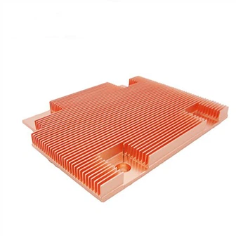
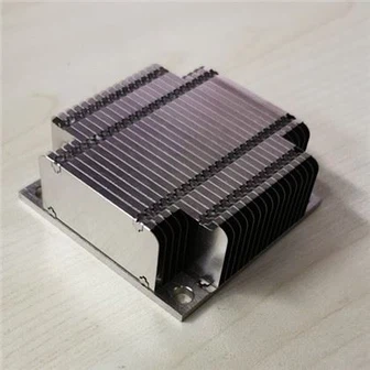
In a package, more than 90% of the heat is dissipated through the package from the top of the chip to a heat sink, usually anodized aluminum-based vertical fins. A thermal interface material (TIM) with high thermal conductivity is placed between the chip and package to help transfer heat. Next-generation TIMs for CPUs include sheet metal alloys such as indium and tin, as well as silver-sintered tin, with conductivities of 60W/mK and 50W/mK respectively.
As manufacturers transition SoCs to chiplet processes, more TIMs with different properties and thicknesses are needed.
YoungDo Kweon, senior director of R&D at Amkor, said that for high-density systems, the thermal resistance of the TIM between the chip and the package has a greater impact on the overall thermal resistance of the packaged module. Power trends are increasing dramatically, especially for logic, so we focus on keeping junction temperatures low to ensure reliable semiconductor operation. Although TIM suppliers provide thermal resistance values for their materials, in reality, the thermal resistance from chip to package (θjc) is affected by the assembly process itself, including the bonding quality and contact area between the chip and TIM. He noted that testing with actual assembly tools and bonding materials in a controlled environment is critical to understanding actual thermal performance and selecting the best TIM for customer qualification.
Gaps are a particular problem. Siemens' Parry said, "The use of materials in packaging is a big challenge. We already know that the material properties of the adhesive or glue, and the way the material wets the surface, will affect the overall thermal resistance presented by the material, that is, the contact resistance. . A lot depends on how the material flows into the surface without creating imperfections that create additional resistance to the heat flow."
05 Dealing with heat issues differently
Chipmakers are looking for ways to solve the heat dissipation problem. Randy White, memory solutions program manager at Keysight Technologies, said: "The packaging method remains the same, if you reduce the chip size by a quarter, it will speed up. There may be some signal integrity differences. Because of the external package keys The bonding wire goes into the chip, and the longer the wire, the greater the inductance, so there's the electrical performance part. So, how do you dissipate so much energy in a small enough space? That's another key parameter that needs to be studied."
This has led to significant investment in cutting-edge bonding research, seemingly focusing on hybrid bonding. But hybrid bonding is expensive and remains limited to high-performance processor-type applications, with TSMC currently one of the only companies offering this technology. However, the prospects for combining photons on CMOS chips or gallium nitride on silicon are promising.
06 Conclusion
The initial idea for advanced packaging is that it will work like Lego bricks - chips developed at different process nodes can be assembled together and thermal issues will be alleviated. But this comes at a cost. From a performance and power perspective, the distance the signal needs to travel is important, and circuits that are always on, or need to remain partially open, can impact thermal performance. Dividing a chip into multiple parts to increase yield and flexibility is not as simple as it seems. Every interconnect in the package must be optimized, and hotspots are no longer limited to a single chip.
Early modeling tools could be used to rule out different combinations of chips, giving designers of complex modules a big boost. In this era of ever-increasing power densities, thermal simulation and the introduction of new TIMs will remain essential.