A Comprehensive Overview of FPGA Thermal Design
For any chip to work, it must meet a temperature range. This temperature refers to the temperature on the silicon chip, which is usually called the junction temperature.
ALTERA's FPGA is divided into two types: commercial grade (commercial) and industrial grade (induatrial). The junction temperature range of commercial grade chips that can work normally is 0~85 degrees Celsius, while the range of industrial grade chips is -40~100 degrees Celsius. In the actual circuit, we must ensure that the junction temperature of the chip is within its acceptable range.

As the power consumption of the chip increases, more and more heat will be generated during work. If you want to maintain the junction temperature of the chip within the normal range, you need to take certain methods to quickly dissipate the heat generated by the chip to the environment.
Anyone who has studied physics in middle school knows that there are three main methods of heat transfer, namely conduction, convection and radiation, and these methods are also used by chips to dissipate heat outward.
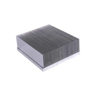
The figure below shows a simplified model of chip heat dissipation. The heat generated by the chip in the figure is mainly transmitted to the outer package of the chip. If there is no heat sink attached, it will be directly dissipated from the chip package shell to the environment; if a heat sink is added, the heat will be transmitted from the outer package of the chip through the heat sink adhesive. to the heat sink, and then to the environment through the heat sink. Generally speaking, the surface area of the heat sink is made quite large, and the contact surface with the air is large, which is conducive to heat transfer. It has been found in usual practice that most of the heat sinks are black, because black objects are easy to radiate heat outward, which is also conducive to the outward dissipation of heat. And the faster the wind speed on the surface of the heat sink, the better the heat dissipation.
Simplified chip heat flow model
In addition, a small amount of heat is conducted to the solder balls of the chip through the chip substrate, and then dissipates the heat to the environment through the PCB. Since the proportion of this part of heat is relatively small, this part is ignored when discussing the thermal resistance of the chip package and heat sink below.
First of all, we need to understand the concept of "thermal resistance". Thermal resistance describes the ability of an object to conduct heat. The smaller the thermal resistance, the better the thermal conductivity, and vice versa. This is somewhat similar to the concept of resistance.

From the thermal resistance of the silicon chip of the chip to the environment, assuming that all the heat is finally dissipated to the environment by the heat sink, a simple thermal resistance model can be obtained, as shown in the figure below:
Chip cooling model with heat sink
The total thermal resistance from the die to ambient is called JA, so satisfies:
JA=JC+CS+SA
JC refers to the thermal resistance from the chip to the external package, which is generally provided by the chip supplier; CS refers to the thermal resistance from the external package of the chip to the heat sink. If the heat sink is attached to the surface of the chip with thermal conductive adhesive, this thermal resistance is to guide the thermal adhesive. Thermal resistance is generally provided by the supplier of thermal conductive adhesive; SA refers to the thermal resistance from the heat sink to the environment, which is generally given by the heat sink manufacturer. This thermal resistance decreases with the increase of wind speed, and the manufacturer usually The thermal resistance values at different wind speeds will be given.
The package of the chip itself acts as a heat sink. If the chip does not have a heat sink, JA is the thermal resistance of the silicon chip to the environment after being packaged. This value is obviously greater than the JA value with a heat sink. This value depends on the characteristics of the package of the chip itself, and is generally provided by the chip manufacturer.
The figure below shows the package thermal resistance for ALTERA's STRATIX IV device. It gives the JA value of the chip at various wind speeds, and these values can be used to calculate the situation without a heat sink. In addition, JC is used to calculate the total JA value with heat sink.

Thermal Resistance of Stratix iv Device Packages
Assuming that the power consumed by the silicon chip is P, then:
TJ(junction temperature)=TA+P*JA
It is necessary to satisfy that TJ cannot exceed the maximum junction temperature allowed by the chip, and then calculate the maximum allowable requirement for JA according to the ambient temperature and the actual power consumed by the chip.
JAMax=(TJMax - TA)/P TA(ambient temperature)
If the JA of the chip package itself is greater than this value, it is necessary to consider adding a suitable heat dissipation device to the chip to reduce the effective JA value from the chip to the environment and prevent the chip from overheating.
In an actual system, part of the heat will also dissipate from the PCB. If the PCB has many layers and a large area, it is also very conducive to heat dissipation.