Intel Launches Next-generation Advanced Packaging Glass Substrates
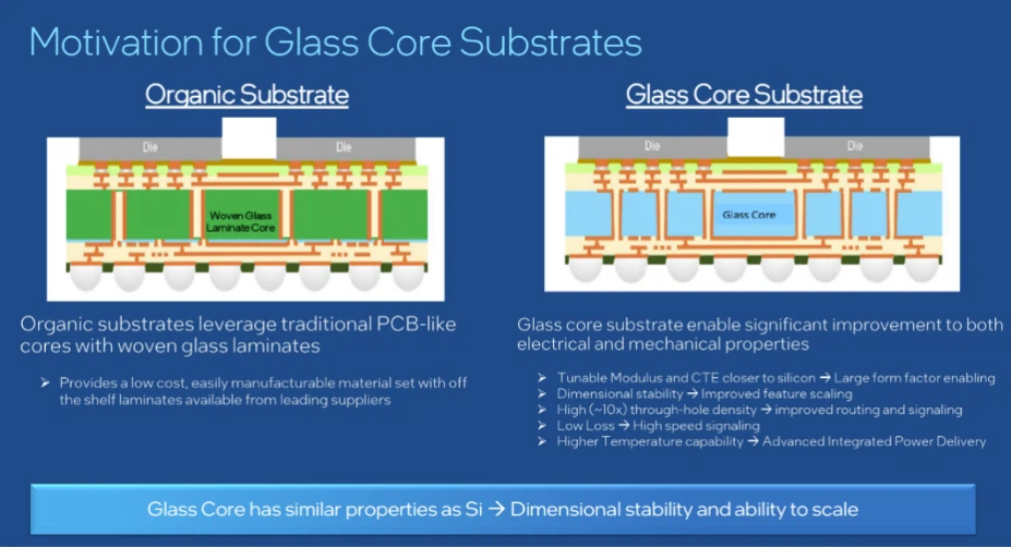
Recently, Intel announced the launch of the industry's first glass substrate for next-generation advanced packaging, planned for mass production from 2026 to 2030. With the inclusion of more transistors in a single packaging, it is expected to achieve more powerful computing power (HashRate) and continue to push Moore's Law limits. This is also Intel's new strategy from packaging testing to compete with TSMC.
Intel claims that the substrate material is a significant breakthrough in solving the warping problem caused by organic substrates used in chip packaging, breaking through the limitations of traditional substrates and maximizing the number of transistors in semiconductor packaging. At the same time, it is more energy-efficient and has more heat dissipation advantages, and will be used in high-end chip packaging such as faster and more advanced data centers, AI, and graphics processing. Intel pointed out that the glass substrate can withstand higher temperatures, reduce pattern deformation by 50%, have ultra-low flatness, improve exposure depth, and have the dimensional stability required for extremely tight interlayer interconnect coverage.
Intel plans to enter the mass production stage from 2026 to 2030, and relevant operators have stated that it is currently in the experimental and sample delivery stages, and the processing stability still needs to be improved. However, the legal entity remains optimistic about the advanced packaging market and believes that the market will grow rapidly. At present, advanced packaging is mostly used in data center chips including Intel, AMD, and Nvidia, with an estimated total shipment volume of 9 million in 2023.


